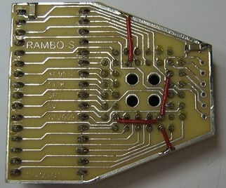
Rambo-S
This project is a small board containing a CPLD and a SRAM IC. It has an SPI interface to utilize the SRAM. The CPLD is used to implement the SPI interface and address the SRAM.
Only four pins are needed; this could be reduced to three if a bi-directional data line was used (like in I2C). It also has an auto-increment function. This means that the address only has to be written once in the initial three byte sequence that also contains the chip select and read/write selection. After these 3 bytes the data can be streamed in or out for any number of bytes. The CPLD is configured in a way that it does not need any external clock. The module could very easily be modified to address 4 (or even more) SRAM ICs with 512Kbytes each which would give 2Mbytes. The CPLD is programmed with the free XILINX ISE 10.1.
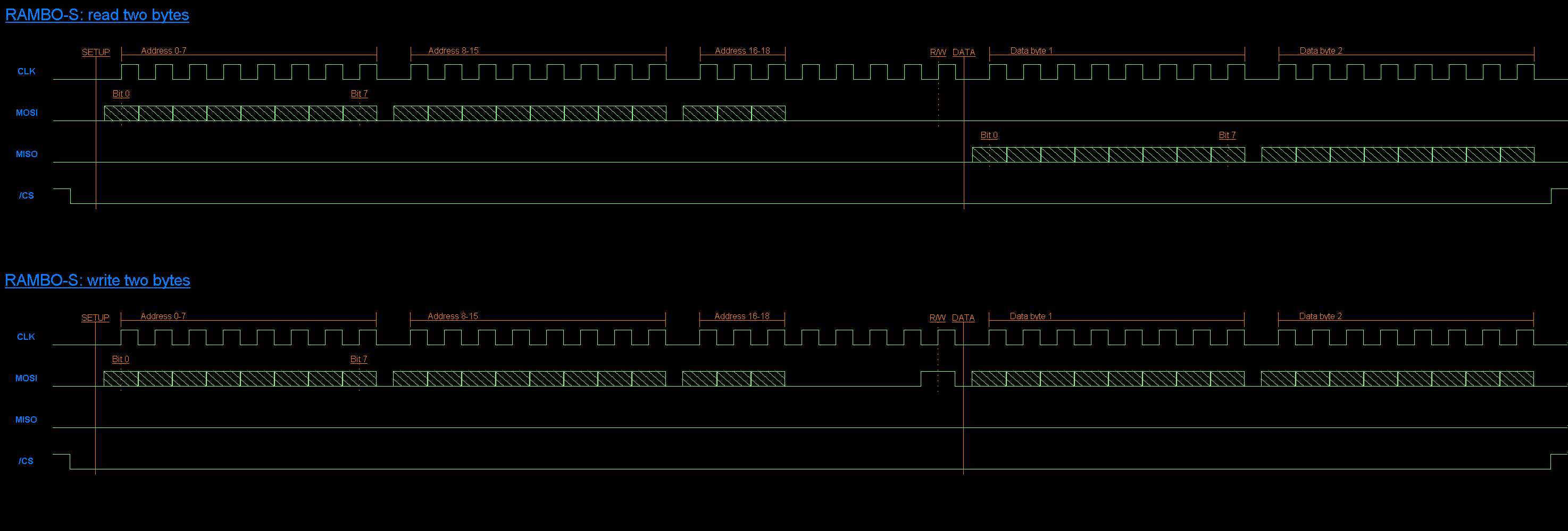
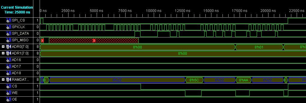
The first 3 bytes contain bits 0-18 of the address and bit 7 of byte 3 is the read/write select (0=read/1=write). After that any number of bytes can be read/written (in the example below two bytes are transmitted). The SPI is in mode CPHA=0, CPOL=0, first bit=LSB. This means that the data is read and written on the rising edge, the data is stable during the change from low to high.
zoom This diagram was made with the program Logic Draw that offers a very simple and fast interface to make neat logic timing diagrams (including an automated signal generator). The PCB layout and the PCB.
The XILINX software provides a test wave generator to simulate and debug the design. This can also be used as a function diagram. These are screenshots of the simulator diagram in XILINX ISE.
zoom
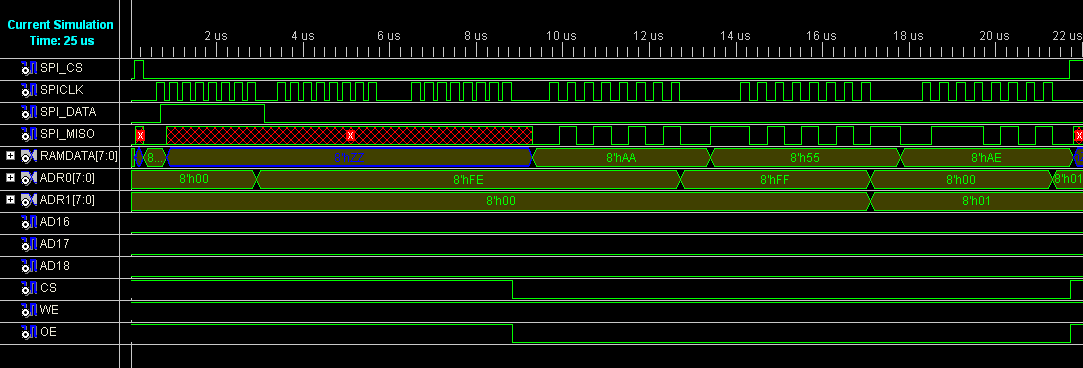
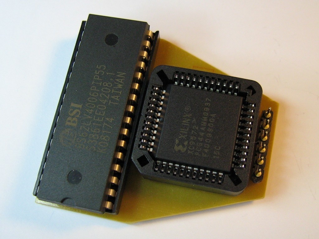
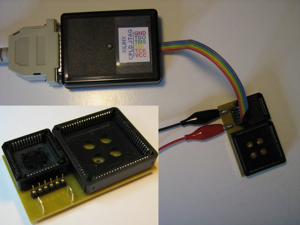
zoom The diagram explains the functionality. During the first three bytes the address is latched with the last falling clock. The address is incremented after each byte. When the counter overflows it jumps back to 0. The ISE project files are not freely available. This is because all other designs I have seen which have this functionality use an external clock and cost money. This is the setup for programming the device. I made a little adapter with JTAG interface for PC44 and PC84 devices. As the simulator and wave generator in the XILINX ISE is very accurate (see diagram above) it is possible to do the entire debugging on the PC. The device only needs to be programmed once and with this little adapter the JTAG header can be spared in the end design.
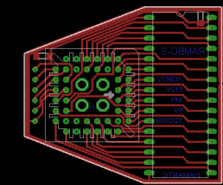
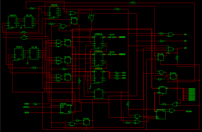
The complete schematic.
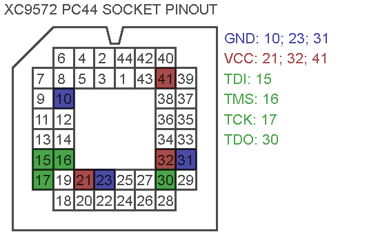
The socket pinout of the XC9572 PC44.